Hi, I have a couple of questions about computer vision.
I have seen this camera and I’m wondering if I can use it to show to it an object, and then show an identical object but with a small difference and the camera has to detect it, is this possible? I also can use an Arduino like Nano 33 BLE Sense or Portenta H7 when available, Raspberry Pi, Google Coral Dev board, Nvidia Jetson Nano, Teensy 4.0, Alchitry Au or Alchitry Cu… Well, the board that it’s necessary.
Thanks to all in advance and I’m sorry if my english is bad
We have plans to build out a deep learning pipeline to make this easy to do this year. The camera hardware can do this… but, the issues is with making CNN networks to do this. It requires a lot of training data which takes a lot of work to collect and then make a network using that data.
Generally no, we have a bunch of shape detectors and color detectors which can be used to do this if the environment is really fixed. Otherwise, you really have to train your own CNN. Everything else is very hard to get working well.
Yes, I have that photos (photo, really) because it would be always from the same perspective (the camera would be always in the same position). Which are these tricks?
I took a photo from internet because I still don’t have the PCB designed, but I can take that as an example. The perspective would be from above and in the future I would like to distinguish between two different PCBs (PCB1 and PCB2 for example) and that OpenMV tells me which is which (or other cam, but I think the best that I have seen is OpenMV)
Thanks and sorry for so many questions and for not giving all the information at once
Okay, so, there’s an algorithm we have called find_rectangles() which will tell you the bounding rect of each pcb. You can pretty easily tell which PCB is there from that if the rect changes.
I kinda need to know what the two different or X PCBs look like. Notice how on the above I’m using the fact that the PCBs are of a different size to tell the difference. If the PCBs look exactly alike except for traces on them then that’s very hard to tell.
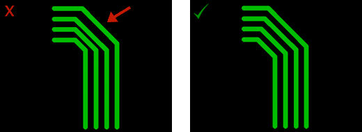
I think I have not explained well, I want to detect errors if I’m making the same PCB all the time I mean with the same form, components, etc. And for example, if the PCB looks like this one: https://i.ebayimg.com/images/g/nJ0AAOSwbYZXZnRS/s-l300.jpg I pretend to find errors like this:
Yeah, I see what you want to do… um, you need extremely high res cameras for that along with a lot of processing power. That’s the job for something in the 10K-100K budget territory…
The OpenMV Cam could technically do it… but, you’d have to scan the camera along the board very slowly taking pics and comparing things. This isn’t really what it is mean for. If with our 5 MP camera coming out we don’t have enough resolution to see that type of detail at all points on the board at once.
Wow 10K-100K… It’s for a school project so you can imagine my budget hahaha
Ok, so I can do, for example, a slow conveyor belt that transport the PCB with the camera OpenMV up and pointing down and the conveyor belt can stop for X seconds every Y seconds so the camera con compare the things, is this right?
As I said it’s for a school project (I should have said it before ) and I don’t have the PCB designed but if it’s easier the PCB can be small.
I knot this forum is for OpenMV, but is there something that can combines with OpenMV or other camera that can do this with low budget? Like Google Coral or Nvidia Jetson Nano, I also can use a Raspberry, teensy 4.0, wait to the new Arduino Portenta H7, etc. Don’t answer this question if it’s against de rules or you don’t want to and really really really thanks!
It’s not really about the processing power. The issues is just that the camera sensor and lens can’t easily make out all the detail.
Mmm, okay, so, our sharpest low noise sensor is our global shutter sensor. You should switch to using that. Once you do so please add a lot of illumination. Then if the PCB fits within view of the camera you are fine. Otherwise, you have to slide the PCB around under the camera.
What you want to do then is map out a few places when you stop the camera over the PCB. Then take pics of those places and store that on the SD card.
Then, when comparing you load those images, use the difference operator to take the difference between the two images. Once you do that you can then look at how many pixels are different and by what amount. If you see large changes then that means there is a defect.
The process that you have to do is the same on all boards you mentioned below. Oh note, your project will require good optical control or it will be very difficult. You’re going to want to find the right lens to use.
Oh I understand, so maybe using other camera with better sensor and lens? Or that cameras are 10-100k?
I think first I need to get more information about computer vision and ML
It’s really about that you need a super high resolution image to see the whole board to the level of detail you want. You should try taking a normal camera and pointing it at a PCB with these issues and seeing if you can see the whole board with the issues clearly. The image you posted online with the defects is taken with a pretty high level of zoom.
I don’t know how big the board you are looking at is. Anyway, again, it’s just about getting a good picture of what you want to work on. If you have a camera and lens optics that can do that then you are fine given the board size and features in the board you are looking for.
